Headline News
01
ETRI Successfully Demonstrates LDM Real-time Broadcasting
Technology in the US


On the occasion of the Regular General Meeting of the Advanced Television System Committee (ATSC), held on May 23rd for two days in Washington, D.C., ETRI, in cooperation with Samsung Electronics, successfully conducted a live demonstration of its multi-channel HD technology. The researchers reproduced an environment of transmitting UHD TV programs, at the broadcasting station, receiving a great response from those concerned. To date, ETRI has demonstrated core transmission technologies on multiple occasions. However, in contrast to previous demonstrations, as in the NAB, which prepared broadcasting images in advance and transmitted the prepared images indoors, this live demonstration transmitted real-time broadcasting programs using the image transmission environment set in the actual broadcasting station.
02
ETRI Receives IEEE Best Paper Award on
UHD Broadcasting Technology


On June 7th, ETRI received the IEEE Best Paper Award in the 13th IEEE International Symposium on Broadband Multimedia Systems and Broadcasting (BMSB 2018), Valencia, Spain. ETRI is honored to be recognized with this award for two years in a row on papers regarding UHD TV broadcasting transmission technology.
The awarded paper is “ATSC 3.0 Physical Layer Modulation and Coding Performance Analysis,” which relates to Layered Division Multiplexing (LDM) technology capable of effectively providing UHD and mobile HD broadcasting programs using a single terrestrial channel. This paper contains the performance analysis results, under actual broadcasting environments, of all modulation and coding combinations provided by the ATSC 3.0 Physical Layer, the next-generation terrestrial broadcasting standard.
03
ETRI Develops the Eyes of AI: Visual Intelligence Chip

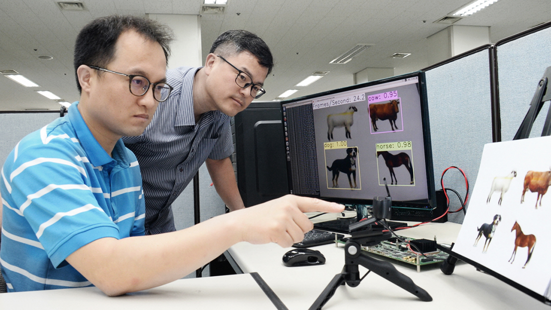
ETRI developed a small-sized, low-power chip capable of processing tens of times larger data than existing chips. This visual intelligence chip is 5mm * 5mm, only half the size of an adult fingernail. The object recognition rate of typical chips using existing software is 1 per second, but the developed chip’s rate is 33 per second. The researchers explained that this computational ability was enabled by connecting 256 neurons. Here, a neuron means a single chip. Also, they emphasized that the core technology was synapse compiler technology, capable of optimizing the neural network without compensating its performance by analyzing the connectivity between a vast number of neural computations and neurons.
The researchers also developed neuron circuit technology, a new type of technology that is aimed at reducing chip energy consumption needed to conduct computation. When equipped with this neuron circuit technology, visual intelligence chips will be able to enable visual intelligence by using only 1/100 of the energy required by CPU and GPU-based chips equipped with existing software. These newly developed visual intelligence chips are capable of efficiently and quickly processing a vast amount of data while consuming less power.


