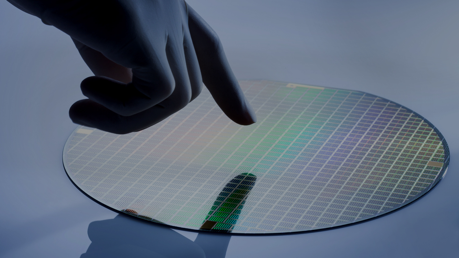
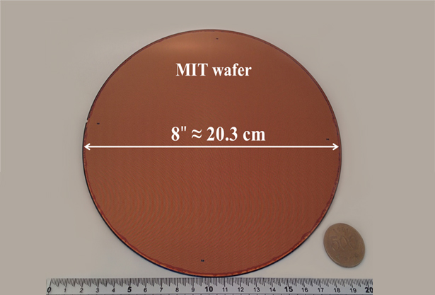
Development of 8-inch wafers for mass-production
By utilizing Mott MIT (metal-insulator transition) since 2005, a team of researchers at ETRI successfully developed technology to mass-produce MIT material applicable to a wide range of sensors.
The MIT phenomenon refers to the switching of an insulator to metal or vice versa without structural phase transformation. The key is the ability to charge electricity to insulators. In 1949, Professor Nevill Francis Mott at the University of Cambridge first suggested the discontinuous MIT theory Later, in 2005, Dr. Hyun-Tak Kim at ETRI verified the theory through experiments.
The existing technology helped to produce devices upon MIT thin films, but two-inch wafers are used to make only 16,000 devices and, since they are designed for experiments, they are expensive with low production output. In order to widely commercialize MIT-using devices, it was necessary to develop technology for large-area wafers. The technology was developed by the ETRI team and it provides the possibility to fabricate at least 200,000 devices on eight-inch size MIT thin film upon the silicon substrates. These eight-inch wafers were manufactured by MOBRIK, to which ETRI transferred its technology. To produce the wafers, the company constructed a fabrication line for eight-inch wafers to produce 100 million MIT devices per month.
This new technology lowers the unit price to produce MIT devices. In particular, since epitaxial thin films have outstanding quality of changing their electrical properties at the MIT critical point, they will mitigate the problem of electric current leakage and reduce the probability of producing faulty or defective devices.
Smart power transistor to be commercialized for various sensors
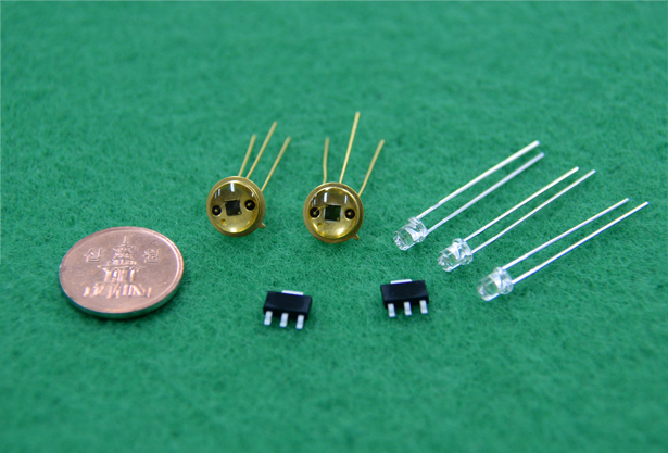
The newly developed technology will help to commercialize Mott MIT devices to be used for household and industrial uses with external parameters such as heat, light, and electricity. The possible applications include critical-temperature sensors and switches, illumination sensors, human body temperature sensors, power transistors embedded with safety circuits, switches for monitoring conducting wires, and sensors to detect human body characteristics.
In the future, the technology is expected to be further used for HTR (high-efficiency power transistors), fire detectors, illumination sensors, power integrated modules, and lithium-ion batteries. Regarding HTR, MIT technology has already been applied to 500,000 LED drivers for illumination as part of commercialization efforts, and also to cardiac pacemakers. In the coming years, the technology will also support commercialization in the automobile motor markets. In addition, the research team aims to raise the domestic share in the markets for fire alarms from the current level of 50% to 90% by the end of 2016 and is pursuing the entrance into overseas markets as well.
The ETRI research team believes that when the new devices are applied for lithium-ion batteries, they will be used for power transistors installed within smartphones and laptops and will be effective for preventing batteries from overheating and swelling. Furthermore, the new technology will be widely utilized in the markets for the human body infrared sensors.
The research results were published in early February 2016 in Applied Physics Letters Materials, an international journal in physics and materials engineering. Dr. Hyun-Tak Kim published his paper in Science in 2007 and was awarded with the King of Invention Award in 2008, Korea’s most esteemed award for patents.
